

Next: Monitoring system
Up: ACC Readout Electronics
Previous: Preamplifier Base Assemblies
Contents
A charge-to-time (QTC) circuit is used to convert the area of the
analog pulses from the FMPMTs to a digital pulses having widths
proportional to the input charges. The leading edge of the QTC output
pulse is the same as leading edge time of its input pulse (plus a
constant offset) so that timing and pulse height information is
encoded in a single pipeline TDC channel. Each QTC board comprises 26
channels, which is the number of FMPMTs in a single  -sector of
the barrel ACC array. Physically the boards are 9U
 400 VME
boards, but the modules do not implement a standard VME interface.
Fig.
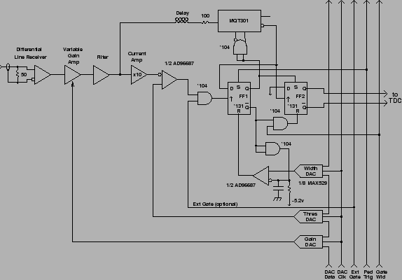
 ![[*]](./icons/crossref.png) is a block diagram of one QTC channel. The
input circuit of the QTC employs a Maxim MAX4144 differential line
receiver. The input of the line receiver can be set to a single-ended
configuration using jumpers, as was done in this case. The next stage
employs an Analog Devices AD603 variable gain amplifier (VGA), which
provides computer controlled gain adjustment over a range of
is a block diagram of one QTC channel. The
input circuit of the QTC employs a Maxim MAX4144 differential line
receiver. The input of the line receiver can be set to a single-ended
configuration using jumpers, as was done in this case. The next stage
employs an Analog Devices AD603 variable gain amplifier (VGA), which
provides computer controlled gain adjustment over a range of  db
to
db
to  db. The VGA stage is followed by a filter circuit which
eliminates high frequency noise.
Figure:
Block diagram of a single charge-to-time converter channel.
 |
The output of the filter amp is routed through a lumped delay line
( ns) to the input of the LeCroy MQT301 charge-to-time
integrated circuit. The MQT301 monolithic is the heart of the circuit
and performs the actual charge-to-time conversion.
The output signal from the filter amp is routed to a second amplifier
and then on to a discriminator circuit based on the Analog Devices
AD96687 ECL comparator. This output from this discriminator is
ultimately used to gate the internal integrator in the MQT301 chip.
The additional gain stage in front of the AD96687 ensures that the
circuit will be sensitive to the smallest signals of interest.
(Signals too small to fire the dicriminator are obviously ignored,
even if they result in a measurable charge at the MQT301 input.) A
pair of ECL flip-flops, a second AD96687 channel, and a collection of
ECL AND gates are used to implement logic circuitry that sets the MQT
gate width and guards against fault conditions caused by input pileup.
Each of the 26 channels on a QTC board has three independent
adjustments: i) a VGA gain setting, ii) a discriminator threshold
setting, and iii) an MQT301 gate-width adjustment. These settings are
controlled using MAXIM MAX529 octal serial DACs. The serial DACs are
set remotely from a computer using a simple serial interface.


Next: Monitoring system
Up: ACC Readout Electronics
Previous: Preamplifier Base Assemblies
Contents
Samo Stanic
2001-06-02
