

Next: Rear-end receiver and digitizer
Up: Electronics
Previous: Electronics
Contents
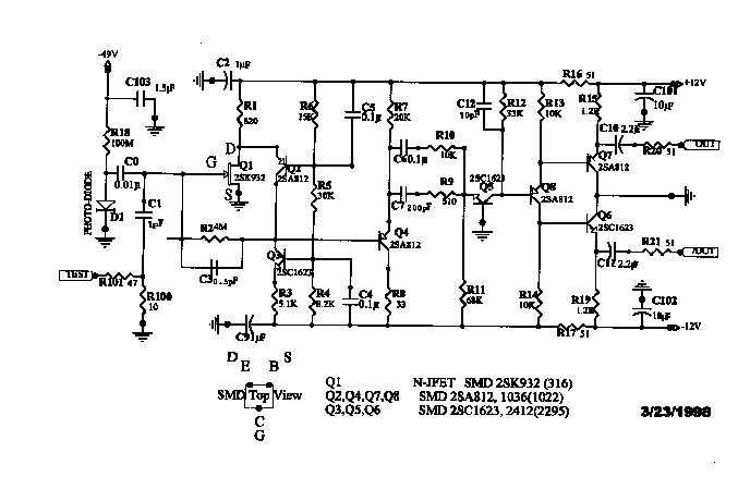
The circuit diagram for the preamplifier and shaper for a photodiode
is shown in Fig. ![[*]](./icons/crossref.png) . The photodiode used is
Hamamatsu S5106. Its active area is 5
. The photodiode used is
Hamamatsu S5106. Its active area is 5  5 mm
5 mm . Scintillation
lights generated in each BGO crystal are collected by two photodiodes
except for the crystals in the two inner-most layers, where only one
photodiode collects lights in each crystal.
Figure:
Schematic diagram of the preamplifier-shaper circuit.
 |
The printed circuit boards (PCB) for the front-end electronics are
stacked together and mounted right behind the rear face of the BGO
crystals. The boards include a board for housing photodiodes and
distributing their biases, a board to house LEDs and to drive them at
each crystal, and a mother board to mount 10 preamplifiers. The rise
time of the signal of the preamplifier and shaper is about 300 ns. The
gain is 6 V/pC and 12 V/pC for the forward and the backward EFC,
respectively.
Signals are sent differentially through a cable of 16
individually-shielded twisted pairs of 16 m in length to the receivers
located outside of the Belle detector. The cable also supplies powers
for preamplifiers and biases for photodiodes, and sends pulses for
pulsing a preamplifier and LED. Each crystal can be pulsed by a light
pulse through fiber cables.


Next: Rear-end receiver and digitizer
Up: Electronics
Previous: Electronics
Contents
Samo Stanic
2001-06-02
