

Next: Double-sided Silicon Detector, DSSD
Up: Silicon Vertex Detector, SVD
Previous: Silicon Vertex Detector, SVD
Contents
A primary goal of the Belle experiment is to observe time-dependent CP
asymmetries in the decays of  mesons. Doing so requires the
measurement of the difference in
  -vertex positions for
  meson
pairs with a precision of
  m. In addition, the vertex
detector is useful for identifying and measuring the decay vertices of
 and
and  particles. It also contributes to the tracking.
Since most particles of interest in Belle have momenta of 1 GeV/
 or
less, the vertex resolution is dominated by the multiple-Coulomb
scattering. This imposes strict constraints on the design of the
detector. In particular, the innermost layer of the vertex detector
must be placed as close to the interaction point as possible; the
support structure must be low in mass but rigid; and the readout
electronics must be placed outside of the tracking volume.
The design must also withstand large beam backgrounds. With the
anticipated high luminosity operation of KEKB, the radiation dose to
the detector due to beam background is expected to be 30 kRad/y at the
full design current. Radiation doses of this level both degrade the
noise performance of the electronics (the readout fails outright at
 kRad) and induce leakage currents in the silicon
detectors. In addition, the beam backgrounds induce large single-hit
count rates. The electronic shaping time--currently set to
1000 ns--is determined by a tradeoff between the desire to minimize
count-rate and leakage current effects, which argue for short shaping
times, and input-FET noise of front-end integrated circuits, which is
minimized with longer shaping times.
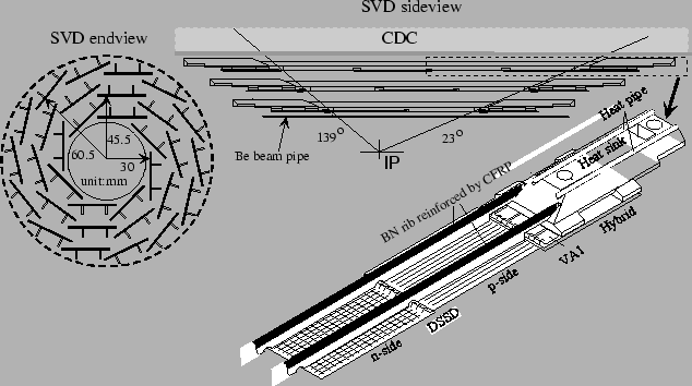
Figure
 ![[*]](./icons/crossref.png) shows side and end views of SVD. It
consists of three layers in a barrel-only design and covers a solid
angle
shows side and end views of SVD. It
consists of three layers in a barrel-only design and covers a solid
angle
 where
where  is the angle from the
beam axis. This corresponds to
86% of the full solid angle. The radii of the three layers are 30
mm, 45.5 mm asnd 60.5 mm. Each layer is constructed from independent
ladders. Each ladder comprises double-sided silicon strip detectors
(DSSDs) reinforced by boron-nitride support ribs. The design uses
only a single type of DSSD, which reduces the cost of detector
production, minimizes the amount of detector development work, and
streamlines testing and bookkeeping during production. The benefit
also extends to hybrid production and ladder assembly, where only a
single type of hybrid is necessary and the design of the ladder
assembly fixtures is greatly simplified.
The readout chain for DSSDs is based on the VA1 integrated
circuit [18]. The VA1 has excellent noise performance (200
e
 e
e /pF) and reasonably good radiation tolerance of
200 kRad. The back-end electronics is a system of flash
analog-to-digital converters (FADCs), digital signal processors
(DSPs), and field programmable gate arrays (FPGAs), mounted on
standard 6U VME boards. DSPs perform on-line common-mode noise
subtraction, data sparsification and data formatting.
Figure:
Detector configuration of SVD.
 |


Next: Double-sided Silicon Detector, DSSD
Up: Silicon Vertex Detector, SVD
Previous: Silicon Vertex Detector, SVD
Contents
Samo Stanic
2001-06-02
