


Next: Hybrid
Up: Front-end Electronics
Previous: Front-end Electronics
Contents
The VA1 chip [18] is a 128-channel CMOS integrated circuit
fabricated in the Austrian Micro Systems (AMS) 1.2- m CMOS
process. VA1 was specially designed for the readout of silicon vertex
detectors and other small-signal devices. It has excellent noise
characteristics (ENC = 200
m CMOS
process. VA1 was specially designed for the readout of silicon vertex
detectors and other small-signal devices. It has excellent noise
characteristics (ENC = 200  + 8 /pF at 1 s shaping
time), and consumes only 1.2 mW/channel.
A block diagram of the VA1 chip is shown in
Fig.
+ 8 /pF at 1 s shaping
time), and consumes only 1.2 mW/channel.
A block diagram of the VA1 chip is shown in
Fig. ![[*]](./icons/crossref.png) . Signals from the strips are amplified by
charge sensitive preamplifiers, followed by
. Signals from the strips are amplified by
charge sensitive preamplifiers, followed by  shaping circuits.
The outputs of the shapers are fed to track and hold circuits, which
consist of capacitors and CMOS switches. Under normal conditions, the
switches are closed and the voltages on the capacitors simply follow
the shaper outputs.
When an external trigger causes the HOLD state to be asserted, the
analog information from all channels is captured on storage capacitors
and then sequentially read using on-chip scanning analog multiplexers.
The multiplexers from the five chips on a single hybrid are daisy
chained and routed to fast analog-to-digital converters (FADCs),
located in the electronics hut about 30 m away from the detector.
Operation of the multiplexer is controlled by a shift register having
one bit per channel. This simple ``track-and-hold'' architecture is
generally well suited to the Belle DAQ system.
Although input-FET noise considerations of VA1 argue for a somewhat
longer shaping time, the shaping time for VA1s is adjusted to 1 s
to minimize the occupancy due to the beam background. Since this time
is shorter than the nominal Belle level-1 trigger latency
(
shaping circuits.
The outputs of the shapers are fed to track and hold circuits, which
consist of capacitors and CMOS switches. Under normal conditions, the
switches are closed and the voltages on the capacitors simply follow
the shaper outputs.
When an external trigger causes the HOLD state to be asserted, the
analog information from all channels is captured on storage capacitors
and then sequentially read using on-chip scanning analog multiplexers.
The multiplexers from the five chips on a single hybrid are daisy
chained and routed to fast analog-to-digital converters (FADCs),
located in the electronics hut about 30 m away from the detector.
Operation of the multiplexer is controlled by a shift register having
one bit per channel. This simple ``track-and-hold'' architecture is
generally well suited to the Belle DAQ system.
Although input-FET noise considerations of VA1 argue for a somewhat
longer shaping time, the shaping time for VA1s is adjusted to 1 s
to minimize the occupancy due to the beam background. Since this time
is shorter than the nominal Belle level-1 trigger latency
( s), a pretrigger signal from the TOF system is used to
assert the VA1 HOLD line until the level-1 signal is formed. If a
level-1 signal does not occur within
s), a pretrigger signal from the TOF system is used to
assert the VA1 HOLD line until the level-1 signal is formed. If a
level-1 signal does not occur within  s, the HOLD line is
deasserted and the system is immediately ready for another event. If
the level-1 does fire, a normal readout sequence ensues.
s, the HOLD line is
deasserted and the system is immediately ready for another event. If
the level-1 does fire, a normal readout sequence ensues.
Figure:
Block diagram of the VA1 chip.
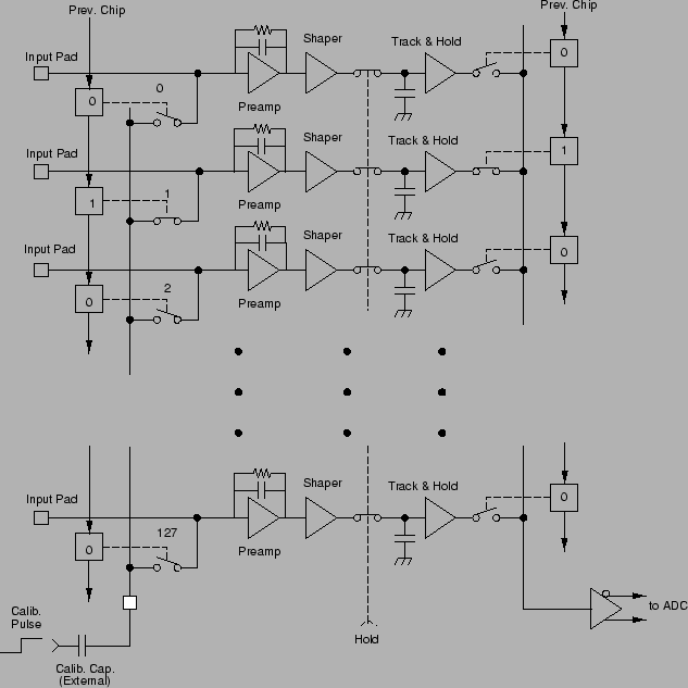 |
VA1 also provides for testing the inputs of individual channels.
This is done by using a shift-register-controlled switching network on
the input side of the chip to sequentially couple an
externally-provided test pulse into each channel. When in the test
mode, the input and output shift registers track on another, allowing
one to observe the shaper output for each channel directly by holding
the hold switches in the track (closed) position. Accurate
calibration can be achieved by using a precision external calibration
capacitor.
Radiation hardness tests of VA1 indicate that it is radiation tolerant
to levels of order 200 kRad. Prior to complete chip failure, a
fractional increase in noise of 1.6 %/kRad was observed. After 150
kRad irradiation the noise level for the  -
- flip sensors
(
flip sensors
( = 29 pF) seems to be marginal.
The detector capacitance, measured noise (ENC, electron noise charge),
and signal-to-noise ratio (S/N) for a normally incident minimum
ionizing particle are summarized in
Table .
= 29 pF) seems to be marginal.
The detector capacitance, measured noise (ENC, electron noise charge),
and signal-to-noise ratio (S/N) for a normally incident minimum
ionizing particle are summarized in
Table .
Table:
Detector capacitance (C), expected noise (ENC) and
signal-to-noise ratio (S/N) at 0 kRad.
| Half-ladder |
Side |
C (pF) |
ENC (e ) ) |
S/N |
| |
p |
7 |
400 |
47 |
S6936  1 1 |
n |
22 |
1000 |
19 |
| S6936 2 |
p-n |
29 |
1100 |
17 |
The dependence of expected S/N on radiation dose is given in
Table .
Table:
Expected signal-to-noise ratio after irradiation.
The radiation dose values shown are for the inner layer.
The radiation doses in the middle and outer layers are assumed to
scale as  .
.
| Half-ladder |
Side |
0 kRad |
50 kRad |
100 kRad |
150 kRad |
| Inner |
p |
47 |
31 |
23 |
18 |
| (1 DSSD) |
n |
19 |
16 |
13 |
11 |
| Middle fwd |
p |
47 |
35 |
28 |
23 |
| (1 DSSD) |
n |
19 |
17 |
15 |
13 |
| Middle bwd |
|
|
|
|
|
| (2 DSSDs) |
p-n |
18 |
16 |
14 |
12 |
| Outer |
|
|
|
|
|
| (2 DSSDs) |
p-n |
18 |
17 |
15 |
14 |
Next: Hybrid
Up: Front-end Electronics
Previous: Front-end Electronics
Contents
Samo Stanic
2001-06-02