

Next: Beam Test by a
Up: Design and Construction of
Previous: Gas
Contents
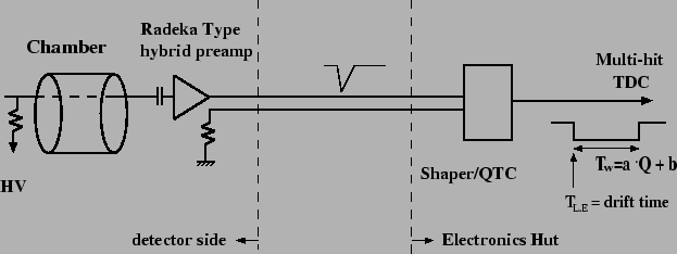
A schematic diagram of the readout electronics of CDC is shown in
Fig. ![[*]](./icons/crossref.png) [37]. Signals are
amplified by Radeka-type pre-amplifiers [38], and sent to
Shaper/Discriminator/QTC modules in the electronics hut via
[37]. Signals are
amplified by Radeka-type pre-amplifiers [38], and sent to
Shaper/Discriminator/QTC modules in the electronics hut via  30
m long twisted pair cables. This module receives, shapes, and
discriminates signals and performs a charge(Q)-to-time(T) conversion
(QTC). The module internally generates a logic-level output, where
the leading edge
  corresponds to the drift time (
 ) and
the width
  is proportional to the input pulse height (
 ). This technique is a rather simple extension of the
ordinary TDC/ADC readout scheme, but allows us to use only TDCs to
measure both the timing and charge of the signals. Since multi-hit
TDCs work in the common stop mode, one does not need a long delay that
analog signals usually require in an ADC readout with a gate produced
by a trigger signal.
Figure:
CDC readout electronics scheme. T and T
and T are the
leading edge and width of the pulse, respectively.
 |
A prototype Shaper/QTC board with 32 channels (VME9U) was fabricated
and tested using a test beam.
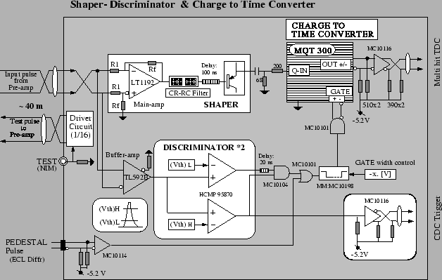
Fig. ![[*]](./icons/crossref.png) shows the schematic circuit of a single
channel. The signals from a pre-amplifier are split into two paths of
circuit; one is an "analog circuit" and the other is a "digital
circuit". The digital circuit provides self-gated signals to the QTC
chip, and trigger output signals. It consists of an amplifier,
comparators, and a gate signal generation circuit. In order to have
good timing resolution without increasing the hit rates for the gate
and trigger signals due to noise signals, we use a "double-threshold
method". The signal from a low-threshold comparator is delayed by 20
ns before forming a coincidence with a signal from a high-threshold
comparator so that the timing of the coincidence signal is determined
by the low-threshold comparator. Threshold voltages are supplied
externally from precisely regulated adjustable voltage power
supplies. We used a fast video-amplifier chip TL592B (Texas
Instruments, USA) for the amplifier and a MAX9687 (Maxim, USA) for the
comparator. An MC10198 (Motorola, USA) mono-stable multi-vibrator
chip was used to produce an ECL-level gate pulse. The gate width was
adjusted by the value of the resistors soldered on the board. The
width was chosen to be
shows the schematic circuit of a single
channel. The signals from a pre-amplifier are split into two paths of
circuit; one is an "analog circuit" and the other is a "digital
circuit". The digital circuit provides self-gated signals to the QTC
chip, and trigger output signals. It consists of an amplifier,
comparators, and a gate signal generation circuit. In order to have
good timing resolution without increasing the hit rates for the gate
and trigger signals due to noise signals, we use a "double-threshold
method". The signal from a low-threshold comparator is delayed by 20
ns before forming a coincidence with a signal from a high-threshold
comparator so that the timing of the coincidence signal is determined
by the low-threshold comparator. Threshold voltages are supplied
externally from precisely regulated adjustable voltage power
supplies. We used a fast video-amplifier chip TL592B (Texas
Instruments, USA) for the amplifier and a MAX9687 (Maxim, USA) for the
comparator. An MC10198 (Motorola, USA) mono-stable multi-vibrator
chip was used to produce an ECL-level gate pulse. The gate width was
adjusted by the value of the resistors soldered on the board. The
width was chosen to be  850 ns in the beam test. We observed
that the jitter of the gate width was 0.5 ns (rms) and the width was
stable within
  1 ns during the beam test.
Figure:
Schematic circuit of the Shaper/QTC board.
 |
The analog circuit provides input signals to the QTC chip. It consists
of an amplifier, a shaping circuit, and a delay. The shaping circuit
has two stages of pole-zero cancellation with time constants of 120
ns/30 ns and 56 ns/20 ns. A passive LC delay line of 100 ns is used
to delay the analog signal to arrive after the leading edge of the
gate. We used an LT1192 (Linear Technology, USA) chip for an
amplifier of the analog circuit because it provides a wider linear
region and better bandwidth than a TL592B.
We set the gains to be 10 and 30 for the amplifiers in the analog and
digital circuits, respectively. These are adjusted by the resistor
values soldered on the board. Since a QTC chip is operated in a
self-gate mode, the charge data are automatically pedestal suppressed
in contrast to the ordinary ADC readout. In order to take pedestal
data, the board takes "pedestal pulses" from the front panel connector
which forces a trigger of the gate circuits of all the channels
without input signals.
For Q-to-T conversion, we used chips recently developed by LeCroy,
MQT300 [39]. The MQT300 chip performs Q-to-T conversion
in three ranges. The conversion gain for the low range is 0.01 pC/ns,
with a factor of 8 and 64 larger conversion gains for the middle and
high ranges. The full range in the specification is  4
4  s
above the pedestals, but the chip provided a good linearity within 1
% deviation up to
  7
7  s above the pedestals. Each range can
be enabled or disabled by the jumper pins on the Shaper/QTC board. In
the beam test, we enabled and recorded all three ranges for a detailed
check of the Shaper/QTC board performance. The MQT300 chip produces
the output pulses as an exclusive OR of the output pulses of the
enabled ranges. When the three ranges are enabled, two pulses are
produced. Since the dynamic range provided by a single range of
MQT300 chips is large enough for the CDC readout application, we plan
to use them only with a single range (middle range) in the actual
Belle experiment.
A beam test was carried out at the  2 beam line of the KEK 12-GeV
PS. Data were taken both with the QTC/multi-hit TDC and the
conventional TDC/ADC readout scheme in order to compare the
performance of two readout schemes directly with the same conditions.
In the QTC/multi-hit TDC scheme case, the output signals from the
Shaper/QTC board are recorded by LeCroy 3377 CAMAC TDC modules. In
the TDC/ADC scheme case the previous beam test arrangement was
used [36]. Spatial resolutions as a function of the
drift distance were measured with various beam conditions. No
significant difference is seen between the two readout schemes and
they are consistent with the previous result.
  distributions
were also measured with the two readout schemes. Again no significant
difference is seen. These results confirm that the new readout scheme
worked successfully and is applicable to the CDC readout.


Next: Beam Test by a
Up: Design and Construction of
Previous: Gas
Contents
Samo Stanic
2001-06-02

