next up previous contents
Next: Beam Test Up: Design and Construction of Previous: Scintillators   Contents

Readout electronics

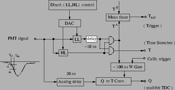
A block diagram of a single channel of the TOF front-end electronics is shown in Fig. [*].

Figure: Block diagram of a single channel of TOF front-end electronics.
\begin{figure}
\vspace{8mm}
\begin{center}
\epsfysize =10cm
\centerline{\psf...
...s,width=15cm,angle=0}}
\vspace{5mm}
\end{center}
\vspace{8mm}
\end{figure}

Each PMT signal is split into two. One is sent to Q-to-T and then to a multihit TDC for charge measurement. The other generates signals corresponding to two different threshold levels: a high level (HL) and a low level (LL). Two LeCroy MVL107s are used for discriminators, with threshold levels set between 0.3$\sim$0.5 mips for HL and 0.05$\sim$0.1 mips for LL. The LL output provides the TOF timing and the HL output provides a trigger signal. HL is used to make a self gate for LeCroy MQT300A Q-to-T conversion and also to gate the LL output. A common trigger is prepared for pedestal calibration of MQT300A. The signal T is further processed in a time stretcher for readout by TDC 1877S. The MQT output Q is a timing signal corresponding to the charge, which is directly recorded with TDC 1877S. Figures [*](a) and (b) show block diagrams of the TOF front-end electronics for (a) event trigger and (b) readout of charge and timing of TOF signals. The gated LL signals from two ends of a counter are mean-timed and coincidenced with the TSC signals to create a fast trigger signal. The nominal coincidence arrangement between one TSC counter and four TOF counters is used to ensure triggers for low momentum tracks. Fig. [*] shows the TSC trigger rates calculated by a Monte Carlo simulation in various coincidence arrangements with TOF counters as a function of discrimination level in units of mips for Bhabha and spent electrons [56]. The time jitter of the signal is smaller than 3.5 ns in each event, and provides a precise event timing to the Belle trigger system to make TDC-stop to CDC and ADC-gate to CsI readout. The time jitter is reduced to 0.5 ns by applying a correction of the hit position in TOF counters.

Figure: Block diagrams of the TOF electronics for (a) trigger and (b) readout.
\begin{figure}
\vspace{8mm}
\begin{center}
\epsfysize =10cm
\centerline{\psf...
...s,width=14cm,angle=0}}
\vspace{5mm}
\end{center}
\vspace{8mm}
\end{figure}

Figure: Event trigger rates due to background photons from Bhabha and spent electrons.
\begin{figure}
\vspace{8mm}
\begin{center}
\epsfysize =10cm
\centerline{\psf...
...s,width=12cm,angle=0}}
\vspace{5mm}
\end{center}
\vspace{8mm}
\end{figure}

The time-stretcher (TS) circuit [57] expands the time difference between the TOF pulse and the reference clock by a factor 20, which enables us to measure the time with a 25 ps precision with the Belle standard 0.5 ns multi-hit TDC readout scheme. The timing of each TOF signal is measured relative to an edge of the reference clock. The time interval T between the TOF signal and the second reference clock edge is measured as shown in Fig. [*]. The output contains an expanded time, where the time interval between the second (trailing) and third (rising) edges represents the time of T expanded by a factor of $f$ (= 20). In this scheme the time interval to be measured is always in the range between 16 ns and 32 ns.

Figure: Time stretcher scheme for TOF.
\begin{figure}
\vspace{8mm}
\begin{center}
\epsfysize =10cm
\centerline{\psf...
...s,width=15cm,angle=0}}
\vspace{5mm}
\end{center}
\vspace{8mm}
\end{figure}

The TS reference clock is provided by an RF clock that is precisely synchronized with the beam collisions. The reference clock with a period of approximately 16 ns can be generated from the RF signal of 508.8875 $\pm 10^{-6}$ MHz, with a time jitter of 20 ps. As the RF clock is used for the whole KEKB timing control, the reference clock is necessarily synchronized with the beam collision timing. A collision bunch number from 0 to 8 is determined in an offline analysis. Due to the small expansion factor of 20 and use of a 16 ns clock, this system provides a virtually dead-time-less TDC (1 $\mu$s). The final TOF information is obtained by applying a time walk correction to the time information. The main parameters for the TOF readout system are summarized in Table [*].

Table: Parameters for TOF/TSC electronics.
Input signal BC408 (Scint.) $\tau_{rise} \sim$ 4 ns (PMT $\sim$ 2.5 ns)
  R6680 (PMT) FWHM $\sim$ 10 ns
    V$_{peak} \leq $ 5 V (1.2 $\sim$ 1.5 V/mip)
    Signal rate $\leq$ 17 kHz at $\geq$ 0.2 mip
Q-to-T MQT300 Self gate (width $\leq$ 100 ns)
    Dynamic range: 0 $\sim$ 500 pC (11 bits)
    Nonlinearity $\sim$ 0.1 %
    Dead time = 5 $\mu$s max.
Discriminator MDC100A Level : 0 $\sim$2 V
  (MVL407S) HL for self gate/trigger
    LL for timing
Mean timer Delay line Input signal width = 30 ns
    Delay = 32 ns
    Time jitter $\leq$ 5 ns
Time stretcher   Clock period = 16 ns (8 RF)
    Expansion factor = 20
    Time jitter $\leq$ 20 ps
    Dead time $\leq$ 1 $\mu$s
Reference time RF clock Total uncertainty $\sim$ 30 ps


next up previous contents
Next: Beam Test Up: Design and Construction of Previous: Scintillators   Contents
Samo Stanic 2001-06-02