

Next: Beam Tests
Up: Design and Construction of
Previous: Calibration by cosmic rays
Contents
At the KEK B factory, a large number of soft  -rays having an
energy of up to a few MeV are generated by spent beam electrons and
positrons hitting the beam pipes and radiation shielding masks. The
dose of the beam induced background in the barrel region has been
estimated to be up to 5 rad/y in the first 2 cm of depth under steady
operation at an integrated luminosity of
 /y. With a
large safety margin, the requirement for radiation hardness is set
such that the light-output decreases to less than 3 %, 10 %, and 20
% at radiation dose of 10, 100, and 1000 rad, respectively.
According to the previous measurements, it was not self-evident
whether our CsI(
 ) crystals would satisfy this requirement.
In order to test the radiation hardness, several full-size crystals
made by each producer were irradiated up to 1000 rad by the  Co
source of 51 TBq at the irradiation facility of Tokyo Institute of
Technology [61]. The irradiation rates were about 3,
3, and 25 rad/min for 10, 100, and 1000 rad irradiation, respectively.
The attenuation length of 1.17 and 1.33 MeV
  -rays from the
 Co source is about 5.4 cm in a CsI crystal.
Irradiation was done in two ways: (a) uniform irradiation in which
crystals were irradiated from the sides of the crystal over the whole
region and (b) front face irradiation in which the sides of the
crystals were shielded and the irradiation was made from the front
surface simulating the actual case. The radiation damage is
restricted in the front region, and approximately 90 % of the total
dose is absorbed in the first 10 cm region out of the total length of
30 cm. The light output of irradiated crystals was measured in two
methods: one with a photomultiplier tube (PM) (Hamamatsu R1847-S) and
a  Cs source, and the other with two photodiodes (PDs)
(Hamamatsu S2744-08, the sensitive area of 10 mm
  20 mm) and
cosmic-ray muons. The latter arrangement is the same as in the actual
Belle ECL.
Two kinds of recoveries of damage after irradiation were observed: (1)
a decrease in the phosphorescence intensity and (2) a partial
restoration of the light output. The intensity of the stray
phosphorescence was too strong to measure the photoelectric peak of
662 keV  -rays immediately after irradiation. After a period of
a few hours to one day the intensity decreased and weakened to the
level at which measurements were possible. In general, the loss of
light-output of a CsI(
 ) crystal after radiation damage partially
recovered.
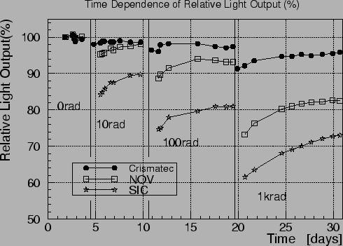
Fig.
 ![[*]](./icons/crossref.png) shows a typical history of light output
measured using a PMT. The light output recovered partially during a
period of about 1, 2, and 4 weeks after irradiation of 10, 100, and
1000 rad, respectively. Unless specifically mentioned, we use the
saturated value of the light output at each dose.
shows a typical history of light output
measured using a PMT. The light output recovered partially during a
period of about 1, 2, and 4 weeks after irradiation of 10, 100, and
1000 rad, respectively. Unless specifically mentioned, we use the
saturated value of the light output at each dose.
Figure:
Time dependence of the light output for uniform irradiation (PMT readout).
 |
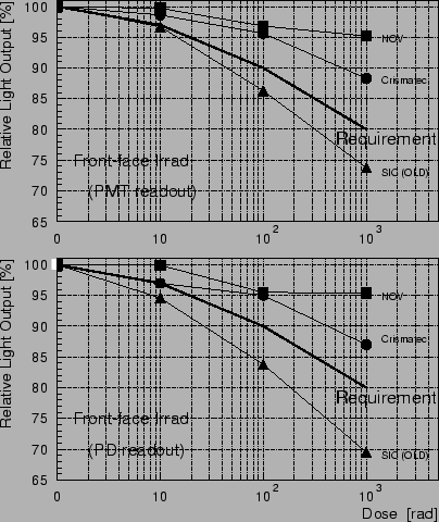
The light output measured with a PMT and PDs as a function of dose for
front-face irradiation is shown in
Fig. ![[*]](./icons/crossref.png) .
The results with a PMT and with PDs agree at a level of a few %. The
figure shows that all of the crystals tested, except for the prototype
made by Shanghai Institute of Ceramics (SIC), satisfy the requirement
of radiation hardness up to 1000 rad. The radiation hardness of SIC
crystals was improved to fulfill the requirement by doping with a
material with the property to cancel the suspicious impurity.
Fig.
.
The results with a PMT and with PDs agree at a level of a few %. The
figure shows that all of the crystals tested, except for the prototype
made by Shanghai Institute of Ceramics (SIC), satisfy the requirement
of radiation hardness up to 1000 rad. The radiation hardness of SIC
crystals was improved to fulfill the requirement by doping with a
material with the property to cancel the suspicious impurity.
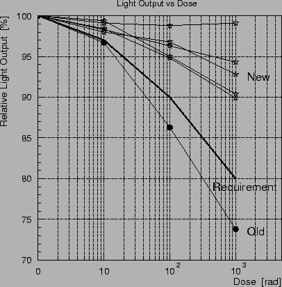
Fig. ![[*]](./icons/crossref.png) shows the results of light output for new
SIC crystals and the original prototype SIC crystals measured using
the PMT readout after front-face irradiation.
shows the results of light output for new
SIC crystals and the original prototype SIC crystals measured using
the PMT readout after front-face irradiation.
Figure:
Light output as a function of radiation dose for front-face
irradiation. The upper and lower figures are the data with the PMT
readout and the PD readout, respectively. The light output values are
normalized to those before irradiation. The thick line represents the
requirement for the radiation hardness of ECL. All crystals, except
for SIC-prototypes, satisfy the requirement.
 |
Figure:
Light output of new SIC crystals versus radiation dose
(front-face irradiation).
 |
The position dependence of the light output measured with PMT and PDs
readouts for uniform and front-face irradiation indicates that the
change in the light output depends little on the position along a
crystal, even for front-face irradiation. This result itself is a
good evidence that the mechanism of scintillation emission in
CsI( ) crystals is little affected by irradiation. We conclude
that only the overall gain factors need to be corrected for the effect
of radiation damage in the running conditions.
The results of studies of the radiation-damage mechanism indicate that
the main cause of radiation damage is due to the degradation in the
attenuation length caused by the formation of color centers, rather
than a deterioration of the mechanism of scintillation light emission.
The coloration of CsI( ) to red or brown was observed after
irradiation. The degree of coloration was correlated with the change
in the light output. The prototype crystals by Shanghai Institute of
Ceramics (SIC) were colored at 100 rad irradiation while those by
Novosibirsk (NOV) and Crismatec were at 1000 rad or beyond. In the
case of the front-face irradiation, coloration was observed in the
front region and the front part of SIC prototype crystals became red
after 100 rad irradiation.
In order to investigate the cause of radiation damage we measured the
spectra of the transmittance, excitation, and emission at 0, 10, 100,
and 1000 rad irradiation with spectrophotometers. Sliced pieces of
5.5 cm  5.5 cm
  2.7 cm in size were used for these
studies. The transmittance was measured across a thickness of 5.5 cm
with the reproducibity of
  1 %. The measurements of the
excitation and emission were made on the surface of each crystal with
somewhat poorer reproducibilities of
  5 %. The results for the
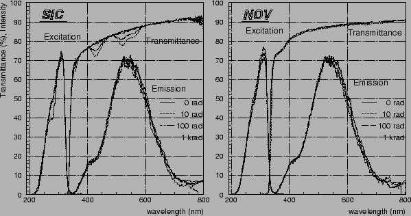
SIC prototype and NOV are shown in
Fig.
 ![[*]](./icons/crossref.png) . Clear absorption bands at around
430 and 520 nm on the transmittance curves can be seen for the SIC
prototype, indicating a formation of color centers. On the other
hand, the deterioration in the transmittance was small for NOV. A
Monte Carlo ray-tracing simulation also supported the idea that the
main result of radiation damage is the formation of color centers.
. Clear absorption bands at around
430 and 520 nm on the transmittance curves can be seen for the SIC
prototype, indicating a formation of color centers. On the other
hand, the deterioration in the transmittance was small for NOV. A
Monte Carlo ray-tracing simulation also supported the idea that the
main result of radiation damage is the formation of color centers.
Figure:
Spectra of the transmittance across a thickness of 5.5 cm and
of excitation and emission at a surface of each crystal after 0, 10,
100 and 1000 rad irradiation for SIC prototype and NOV. The
transmittance data were corrected for the reflection loss at the
surfaces. Clear absorption bands are observed on the transmittance
curve for the SIC prototype. The spectra of excitation and emission
were corrected for wavelength dependence of the quantum efficiencies
of PMT.
 |


Next: Beam Tests
Up: Design and Construction of
Previous: Calibration by cosmic rays
Contents
Samo Stanic
2001-06-02
