next up previous contents
Next: Calibration by cosmic rays Up: Design and Construction of Previous: Mechanical assembly   Contents

Readout electronics

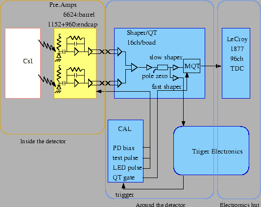
A block diagram of readout electronics is shown in Fig. [*]. Each CsI($Tl$) counter is read out by an independent pair of silicon PIN photodiodes (Hamamatsu S2744-08) and charge sensitive preamplifiers [60] attached at the end of the crystal. The preamplifier output is transmitted on about 10-m long, 50 $\Omega$ twisted pair cables to a shaping circuit where the two signals from the same crystal are summed. The summed signal is then split into two streams: one for the main data acquisition for energy measurements and the other for the trigger electronics. The main signals for energy measurements are shaped with a $\tau = 1 \mu$s time constant and fed into a charge-to-time (Q-to-T) converter, LeCroy MQT300A, installed on the same card. The output of Q-to-T converter is transmitted via twisted pair to a TDC module, LeCroy 1877S multi-hit TDC module, in the electronics hut for digitization. The trigger signal is shaped with a shorter time constant and $\sim$16 lines are combined to form an analog sum for the level-1 trigger.

Figure: Block diagram of the ECL readout electronics.
\begin{figure}
\vspace{3mm}
\begin{center}
\centerline{\psfig{file=picture_4/...
...s,width=12cm,angle=0}}
\vspace{3mm}
\end{center}
\vspace{3mm}
\end{figure}

The specifications for the large-size silicon PIN photodiode are listed in Table [*]. An improved version (S2744-08) of Hamamatsu photodiodes with higher quantum efficiency satisfies the above specifications. Each photodiode was burned in before shipment at 80$^o$C for 50 hours with 70 V bias voltage applied.

Table: Photodiode specifications.
Sensitive area 10 $\times$ 20 mm$^2$
Wafer thickness 300 $\mu$m
Applied high voltage $\leq$ 70 V
Capacitance Average $\leq$ 85 pF,   max $\leq$ 105 pF
Sensitivity ($\lambda$ = 560 nm) Average $\geq$ 320 mA/W,   min $\geq$ 310 mA/W
Temperature dependence $\leq$ 0.01 %
Dark current Average $\leq$ 4 nA,   max $\leq$ 15 nA
Temperature dependence Average $\leq$ 10 %/$^o$C
Radiation hardness At 6 Gy At 68 Gy
Change of dark current $\leq$ 8 % $\leq$ 40 %
Change of capacitance $\leq$ 0.4 % $\leq$ 1 %
Change of sensitivity $\leq$ 0.3 % $\leq$ 0.3 %

We performed a photodiode endurance test by keeping 160 units of S2744-03 photodiodes with a 60 V reverse bias at a temperature of 60$^o$C for 4000 hours. The typical dark current at 60$^o$C is 300 nA. The dark current of each photodiode was measured at room temperature several times during the test and the average values of these measurements are about 3.2 nA. The dark current of 160 pieces was very stable and no photodiode showed a large increase.
A unit of two-channel preamplifiers consists of two hybrid chips and a mother board installed in an aluminum shielding case [60]. An extensive performance test was carried out for 100 pieces of preamplifiers produced. The test result was quite satisfactory.
The readout electronics was calibrated with 60 keV $\gamma$-rays from a $^{241}$Am source. The photon absorbed with the PIN diode depletion layer produces 16,600 electron-hole pairs. That allowed to calibrate the electronics in units of photoelectrons.
next up previous contents
Next: Calibration by cosmic rays Up: Design and Construction of Previous: Mechanical assembly   Contents
Samo Stanic 2001-06-02